Overview
Through the addition of high-precision alignment capabilities for extremely precise placement of printed structures, Quantum X align improves Nanoscribe’s field-proven 3D Microfabrication technology based on Two-Photon Polymerization (2PP).
With this highest resolution 3D printer’s nano precision aligned 3D printing capabilities, users can print freeform micro-optics with submicron accuracy directly onto optical fibers or photonic chips.
Create effective optical interconnects for photonic packaging, integration, or miniature imaging optics, such as those used in endoscopy to perform minimally invasive surgery.
Video Credit: Nanoscribe
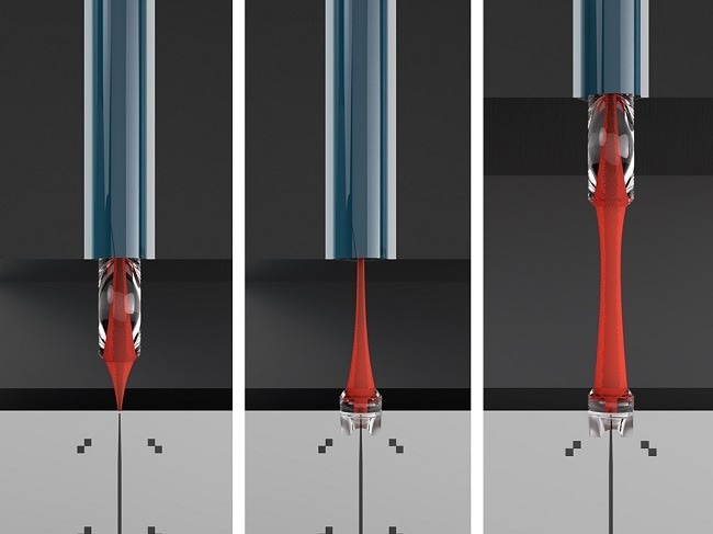
It is laborious to place and actively align the various microoptical elements to one another when packaging integrated photonic circuits (PIC) or miniature medical devices. This procedure is made simpler by Quantum X align.
The spatial orientation of optical interfaces on photonic chips or fiber cores is automatically determined, and freeform microoptics or diffractive elements are printed in place directly while accounting for tilt.
As a result, assembly tolerances are eased, the process chain complexity is decreased, and even more compact devices are made possible. It is no longer necessary to use the frequently expensive active alignment.
Precision alignment and the lowest coupling losses are ensured when printing onto single-cleaved fibers or v-groove fiber arrays with the automatic 3D fiber core detection system and automatic tilt correction.
A confocal imaging module is another feature of Quantum X align that allows for fully automatic 3D alignment to predefined markers or waveguides and also 3D mapping of substrate topographies.
For 3D printing microoptical components directly onto surfaces or facets of photonic chips and consequently for photonic packaging processes in industrial manufacturing, Quantum X align is the ideal 3D-aligned nanofabrication tool.
Features
- 3D printing on chips: Using 3D substrate topography mapping, precisely aligned printing can be done on the chip’s surface or a specific facet
- Smart slicing for high-speed microfabrication
- High-performance direct laser writing with automatic precision alignment
- 3D printing on fibers: Precisely aligned printing on the facets of optical fibers based on fiber core detection
- 3D alignment: Automatic detection and compensation of substrate tilt in three rotation axes
- On fibers and on chips
- Hardware and workflows that are optimized to print on fiber arrays and photonic chips that can be customized or standard
- Nanoprecision 3D alignment
- Nanoprecision measurements of substrate topography and 3D alignment on chips and fibers
- Optical grade 3D-printing
- Advanced freeform microoptics with the highest shape accuracy and surface roughness of ≤10 nm
- High-precision fiber core detection based on fiber illumination unit
- High-precision 3D printing of microoptical elements onto fiber arrays and chips
- Automatic substrate tilt recognition and print adjustment in three rotation axes
- Confocal module for 3D topography detection and precise alignment on chip and chip facets
- Automatic alignment system with nanoprecision in all spatial directions
- Automated self-calibration routines for accurate laser power control and positioning
- Smart slicing for optimized resolution, precision, and speed
- Touchscreen and remote-control software ensure high usability
- Substrate holders for customized or standard fiber arrays and photonic chips
Application areas
- High-precision 3D printing based on Two-Photon Polymerization (2PP)
- Aligned 3D printing at predefined positions
- Feature size control down to 100 nm
- Easy and robust setup with Dip-in Laser Lithography (DiLL)
- Rapid prototyping and high-performance small-series manufacturing of precisely aligned freeform microoptics
- Optical interconnects on integrated photonic chips
- Lensed fiber arrays for optical interconnects
- Beam shaping or light collection on integrated photonic chips
- Imaging and beam shaping optics on single fibers or fiber arrays
- Developed for trailblazers and creative thinkers in research and manufacturing in:
- Integrated photonics
- Optical sensing
- Quantum technology
- Photonic packaging
- Medical instrumentation
Free space microoptical coupling
Different types of fiber to chip Free Space Microoptical Couplers (FSMO). Renderings of a) lensed fiber to chip, b) lensed chip to fiber and c) lensed fiber to lensed chip. Image Credit: Nanoscribe
- For photonic packaging and integration, Free Space Microoptical Coupling (FSMOC) provides a very reliable and effective light coupling solution
- Customized beam shaping and mode field adjustments are made possible by freeform microoptics that are made directly on the optical interface of chips or fibers
- Eliminates the need for active alignment, such as when fabricating optical interconnects, and results in loosened alignment tolerances between optical elements
- FSMOC is adaptable in use and is simple to customize to meet the needs of individual applications. Even earlier chip-level mode field adjustments can be applied to the new 3D printing method
- Cost-efficient photonic packaging strategy
- Relaxed alignment tolerances for passive alignment
- Achievable coupling losses down to ≤1 dB
- Easy and quick adaption to new requirements and applications
Rendering of a lensed fiber to lensed chip array vs. a microscope image of a 3D printed lensed fiber array (LFA). The microscope image clearly demonstrates how precise the optical projection of lensed fibers is. Here, green light is collimated into parallel light beams. Sample of the research project MiLiQuant. Image Credit: Nanoscribe
Rendering and print of mode field shaping microoptics aligned and printed with submicron precision onto the facet of a photonic chip. Sample of the research project HandheldOCT. Image Credit: Nanoscribe
3D printing precisely aligned on an AFM cantilever and SEM image of the final, decorated cantilever structure. Image Credit: Nanoscribe
Specifications
Benchmark scores
Table 1. Source: Nanoscribe
| . |
. |
| 3D alignment precision 1 |
down to 100 nm (xy) / 500 nm (z) |
| Surface roughness Ra |
down to ≤ 10 nm |
| Shape accuracy Sa |
≤ 200 nm (ISO 25178) |
| Feature size control 2 |
down to 100 nm |
| Typical processing time |
20 min for 8x lensed fiber array |
| Achievable coupling losses 3 |
≤ 1 dB |
General system properties
Table 2. Source: Nanoscribe
| . |
. |
| Printing technology |
3D printing based on Two-Photon Polymerization (2PP)
Dip-in Laser Lithography |
| Substrates |
Fiber arrays (v-groove)
Single cleaved fibers (single-/multimode)
Photonic chips (unmounted/TO can)
Wafers from 1” to 6” (25.4 mm to 150 mm)
Glass, silicon, other transparent and opaque materials
Further form factors on request |
| Photoresins |
Nanoscribe IP Photoresins (polymers printing)
Open for third-party and custom materials |
| Maximum print area |
50 x 50 mm² |
Given values may vary depending on the photoresin and structure geometry.
1 Detection accuracy depends on selected method
2 100 nm feature size control in all spatial directions
3 Best case for typical applications, depending on design, substrate quality and measurement method
We are confident in Nanoscribe’s new, aligned 3D printing technology for producing lensed fiber arrays and lensed chips with virtually limitless optical designs.”
Joost van Kerkhof, Chief Operations Officer, PHIX Photonics Assembly
Align the print job with the software
Simple but powerful workflow
Video Credit: Nanoscribe
- The Quantum X align interface is simple to use. Utilize the cutting-edge PC software to prepare the print job while enjoying the intuitive user interface
- Specify the substrate and alignment techniques to be used and import user’s designs as STL files
- Standard structures and materials have print parameters that can be customized for the application and are readily available out of the box
- In a short amount of time, evaluate new applications with test runs on plain wafers and parameter sweeps
- Easy to setup
- Cleaved single fibers, fiber arrays, and photonic chips can all use substrate holders from Quantum X align that are adaptable. Substrates can be loaded one at a time or in groups
- Since there is no need for spin-coating or oil-immersion setups, the process itself benefits from the simplicity of Nanoscribe’s Dip-in Laser Lithography technology. Liquid photo resin is applied to the substrate and the objective lens dips directly into it
- Start the print job via the touchscreen
- Users can easily complete a successful print job with Quantum X align’s intuitive touchscreen menu
- Start the print job after registering the starting positions on each substrate and making sure everything looks correct using the high-resolution live camera view
- Depending on the configuration, the system will then carry out submicron alignment automatically
- After printing, the leftover resin is simply rinsed with organic solvents to remove it. Thermal treatment, as is known from other lithography technologies, is not required
- This guarantees the highest level of compatibility with the current process chain and prevents harm to the optical devices on the chips
- Stay connected with nanoConnectX
- With the remote access software nanoConnectX, start and keep an eye on the print job from the office
- The Quantum X system is prepared for use in multi-user settings and in production settings
Workflow facts
Software-based workflow
- The software is specially made for producing intricate print jobs requiring tasks requiring nanoprecision alignment
- Import the .stl files, then choose the substrate parameters, printing, and alignment strategies for fiber, photonic chips, or any other substrate topography that has been specified. Print jobs can be sent over a network connection to Quantum X align
Benchmark scores
Table 3. Source: Nanoscribe
| Key features |
Benefits |
| 3D CAD model import |
Intuitive workflow generates suitable print job files from standard STL or OBJ files |
| Print parameter presets |
Ready-to-use preset parameters to achieve optimal printing results on fiber arrays or photonic chips |
| Alignment parameter presets |
Parameters for standard v-groove fiber arrays, and typical waveguides on photonic integrated circuits are available out of the box |
| 3D print preview |
Avoid mistakes and get immediate feedback |
| Smart slicing |
Print with the resolution that your design requires: Optical grade surface finishes with highest resolution and coarsely written support structures in one print file |
Touchscreen
- Utilize the Quantum X align front panel touch screen and the graphical user interface to control and monitor the system (GUI)
- It directs users to a successful print. After choosing the print project, load the substrate and then begin printing
Table 4. Source: Nanoscribe
| Key feature |
Benefits |
| Three live cameras |
Monitor the printing process online from three perspectives and always be up to date on the current status of your print job |
| Stage control in x, y and z direction |
Move the stage to any position on the substrate to define your print area |
| User-friendly print setup |
Select resin and substrate, and start the print job with just one click |
| Project list |
Keep track of the entire print job history |
| Automatic interface finder |
Identify the interface of the substrate with submicrometer accuracy |
| Coarse alignment |
Register the coarse initial position of the substrate with a tap on the touchscreen, for subsequent automatic alignment |
nanoConnectX
- The Quantum X systems’ remote access software is called nanoConnectX. It gives any online-connected computer all the touchscreen’s features and display capabilities
Table 5. Source: Nanoscribe
| Key feature |
Benefits |
| Remote access to the system |
Connect Quantum X align to your computer, no matter where you are |
| Use all features of the touchscreen |
Prepare, control and monitor your print jobs from any location |
| Upload and download print jobs and reports |
Take advantage of a direct access from your computer to print-related files |
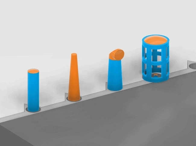
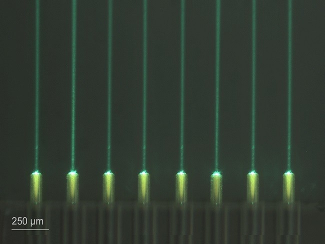
Array of freeform microoptics aligned and printed on individual fibers in a v-groove fiber array. Explore unlimited design freedom. Image Credit: Nanoscribe
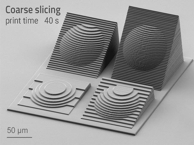
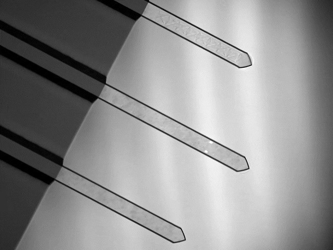
SEM of an optical lens printed onto an angled support structure. With the new smart slicing feature, you can print optical grade surfaces and coarsely written support structures in one process step. Image Credit: Nanoscribe
Rendering of a photonic chip. The confocal module allows for 3D alignment to chip features and dedicated markers. Image Credit: Nanoscribe