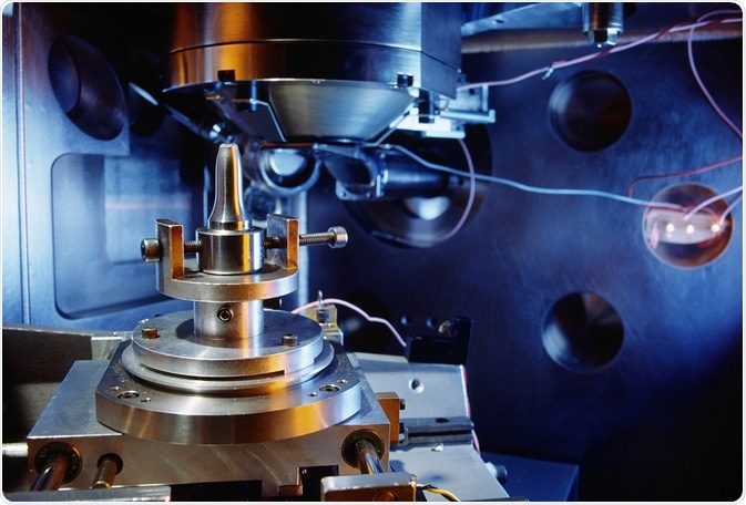
A scanning electron microscope (SEM) generates magnified images of the surface of samples of interest via a beam of fast-moving electrons to in place of the light used in a conventional microscope, to ‘shine’ onto the sample.

Image Credit: Bildagentur Zoonar GmbH/Shutterstock.com
SEM uses the beam of electrons within vacuum conditions to interact with the surface atoms of a sputter-coated sample, commonly with gold or other suitable metals, this produces multiple electron signals; reflected electrons, secondary electrons, transmitted electrons as well as light, X-rays and an absorbed current.
These secondary electrons are localized, and these are detected to obtain high resolution, high magnification surface images. As a result, the image which can be produced is 10 to 200 times larger, generating images that allow for analysis of the sample topography, morphology, and composition.
The ability of SEM to produce images of samples with such a high magnification while retaining a high resolution has resulted in SEM being established in a vast amount of applications across industrial, commercial, and research sectors.
Life sciences
SEM is utilized in several fields of biological science such as; cell and molecular biology for investigating cell morphology, microbiology investigating bacteria and viruses and their interactions with surfaces, each other and other cells.
SEM has allowed for the investigation of cell reactions to cryopreservation, allowing for the development of appropriate media for cryopreservation, while minimizing damage from rapid freezing. SEM has been useful for exploring effects of antibiotics in bacterial morphology and ultrastructure to enhance understanding of their mechanism of action.
Localizing specifically tagged proteins in mitochondria has been made possible via SEM. In medicine, SEM has been used to explore tissue and cells and can facilitate diagnosis of disease.
In forensic science, SEM is utilized to analyze trace evidence such as gunshot residue, hairs, fibers, glass paint fragments, and fingerprints. SEM can be used to investigate the factors that lead to a death, including analysis of the soil surrounding a body or damaged tissue.
Materials science
The high resolution, incredibly magnified images in SEM are useful within materials science to test the quality of materials ensuring that they are fit for purpose and can be used in predicting and preventing material failure.
Research into the design of new materials is dependent on gaining a deeper understanding of the new material and its properties via close observation.
Industries such as aerospace, electronics, chemistry, and energy rely on SEM when developing innovative materials.
Recently, there have been developments in the use of nanowire for creating new, sensitive, gas sensors. SEM plays a major role in these developments, permitting the characterization of nanowires and further understanding of their behavior to improve on existing methods of creating gas sensors.
Semiconductor sciences
Detailed topographical information is vital to developing high performing semiconductors. Therefore, SEM is used within this field to give fast and accurate measurements of the composition of semiconductors.
Other wafer manufacturing processes rely on SEM, which are one of only three essential quality control tools that are used in these processes.
New electronics devices are reducing in size; this has led to a necessity for SEM investigation into the effectiveness of new production and fabrication methods in the construction of these tiny electronics.
As the need for electronics in our everyday lives continues to grow, alongside the boom of the Internet of Things (interrelated computing devices that have unique identifiers and can communicate information without the need for human interaction such as smart home devices), product designers are striving for ways to make devices more intuitive, cost-effective, and power-efficient.
Studying the microchips and materials used in these devices can give key insights into these important factors.
References:
- Basu, S. (2006). Scanning electron microscopy in forensic science. Encyclopedia of Analytical Chemistry: Applications, Theory, and Instrumentation.
- Carr, K. (1971). Applications of Scanning Electron Microscopy in Biology. International Review of Cytology, pp.183-255.
- Chen, X., Ren, L., Zheng, B., & Liu, H. (2013). Physics and engineering aspects of cell and tissue imaging systems: microscopic devices and computer-assisted diagnosis. Studies in health technology and informatics, 185, 1-22.
- Cushnie, T. T., O’Driscoll, N. H., & Lamb, A. J. (2016). Morphological and ultrastructural changes in bacterial cells as an indicator of the antibacterial mechanism of action. Cellular and molecular life sciences, 73(23), 4471-4492.
- Hornyak, G. L., Tibbals, H. F., Dutta, J., & Moore, J. J. (2008). Introduction to nanoscience and nanotechnology. CRC press
- Morris, G. J., Goodrich, M., Acton, E., & Fonseca, F. (2006). The high viscosity encountered during freezing in glycerol solutions: effects on cryopreservation. Cryobiology, 52(3), 323-334.
- Perkins, G. A. (2014). The use of miniSOG in the localization of mitochondrial proteins. Methods in enzymology (Vol. 547, pp. 165-179). Academic Press.
- Wu, G., Choi, E., Chu, P., Dinescu, G., Jung, R. and Zhao, Y. (2018). Recent Applications of Scanning Microscopy in Surface Engineering. Scanning, 2018, pp.1-2.
Further Reading
Last Updated: Mar 18, 2020