Hitachi’s latest TM4000 II benchtop SEM makes advanced electron microscopy fast and simple for all users. It enables large depth-of-focus imaging, high contrast, high resolution, and rapid detection of the distribution of chemical elements with minimal time for sample preparation. Users can effortlessly image and examine any specimen in minutes.
Key capabilities
- Compositional difference in samples can be quickly detected with the Backscatter Electron (BSE) detector
- Clear topographical contrast can be observed with the specialized Secondary Electron (SE) detector
- Voltage control (up to 20 kV) and probe current control rapidly improve results
- High-resolution imaging with magnification ranging from 25x to 250,000x
- The X-ray microanalysis (EDX) capability (option), including fast mapping*, provides a better understanding of chemicals
- Specimens can be rapidly navigated with the built-in navigation camera and motorized stage*
- Multiple or large specimens can be analyzed due to the large stage and chamber (specimens measuring up to 50 mm in height and 80 mm in diameter)
- Charging concerns on electrically insulating samples can be eliminated by switching the vacuum mode with just one click
- In-situ dynamic experiments can be observed with compression or tensile, electrical probing, cooling, heating, and nanoindentation sub-stages*
- Sophisticated detection capabilities, such as STEM or Cathodoluminescence* can be added
- Quantitative surface metrology data can be directly obtained in the SEM*
- Microscopy and data analysis can be automated with options for multi-field acquisition as well as automated particle and phase analysis*
*Options
Flexible imaging made easy
The TM4000 II benchtop SEM keeps time-to-date and usability at its heart, but not at the cost of the flexibility required by users to truly interpret their specimens. Users can select between BSE (compositional contrast) and SE (surface contrast) on both insulating and conductive specimens without previous sample preparation.
Both BSE and SE detectors can be visualized simultaneously (either mixed or separately) and also in low-vacuum mode. The potential to choose suitable acceleration voltage and probe current helps guarantee optimum results.
Left: Chemical contrast (BSE); Middle: Topography (SE); Right: Mixed SE/BSE image. Image Credit: Hitachi High-Tech Europe
Fast navigation
With a fully incorporated navigation camera, users can rapidly find their way around their sample. Users can effortlessly overlay and correlate their optical and SEM images to know exactly where they are and what they have done at all times.
The left side shows an SE image of the inside of a watch, bottom right shows the optical image with overlayed SEM images from areas that have been imaged. Image Credit: Hitachi High-Tech Europe
High-performance for advanced elemental analysis
The built-in X-ray microanalysis (EDS) system from prominent suppliers, such as Bruker or Oxford Instruments, guarantees precise and rapid elemental analysis with sophisticated features that are present in other benchtop SEMs. Real-time peak deconvolution makes sure that spectral line overlaps are eliminated to offer real elemental distribution and thus prevent inadvertent misinterpretation.
Line overlap with W and Si peaks in the spectra on the right. By using peak deconvolution, it is possible to see which grains actually contain W. Image Credit: Hitachi High-Tech Europe
Automate particle, fiber, or chemical analysis
Users can enhance their statistics and remove time-intensive work by adding Hitachi’s robust modules to automate their matrix, fiber, or particle analysis (a capability usually associated only with full-size SEMs).
Completely automated acquisition and analysis in the TM4000 II benchtop SEM allow users to rapidly define morphology, size, and chemical composition, even across an unlimited number of features. This potential can be crucial in defining materials such as:
- Metal powders for additive manufacturing
- Electrospun fibers
- Identification, liberation, and characterization of the mineral phase
- Steel cleanliness (to ISO4967 standard)
- Technical cleanliness (to ISO16232/VDA19 standards)
- Asbestos analysis (to VDI 3492/ISO14966 standards)
Left: Automatic particle detection. Right: Particle size distribution. Image Credit: Hitachi High-Tech Europe
Mineral particle identification and characterization using Bruker AMICS. Left: BSE image; Middle: Identified particles; Right: Mineral classification. Image Credit: Hitachi High-Tech Europe
Automated fiber thickness measurement. Image Credit: Hitachi High-Tech Europe
Examine wide areas automatically
Modules for fully-automated wide-area acquisition and stitching (such as chemical analysis and imaging) allow users to get all their required high-resolution data, even across large-length scales.
Geological thin section stitched using 3 x 3 images to cover a 6 x 5 mm area. Image Credit: Hitachi High-Tech Europe
Quantitative surface metrology
Material surfaces can be fully interpreted with built-in, tilt-free 3D surface modeling and metrology. Surface parameters, like roughness, angle, or depth, including 3D surface textures explained in ISO 25178, can be measured.
3D surface roughness of a worn metal surface. Image Credit: Hitachi High-Tech Europe
Cathodoluminescence detector
The built-in cathodoluminescence detector can spot the light produced from a wide range of pharmaceutical, geological, and semiconductor materials in response to electron beam irradiation. This can serve as a robust tool in identifying active pharmaceutical ingredients (API) in pharmaceutical specimens or to perform geological studies, such as growth history and crystal zonation.
Sample: Coarse-grained Syenite with zonation in the alkali feldspar. Left: CL image; Middle: BSE image; Right: Mixed CL and BSE. Small variations in Ca and Na content create CL contrast, hardly visible in the BSE image. Image Credit: Hitachi High-Tech Europe
SE, BSE, and CL images of a pharmaceutical powder. Image Credit: Hitachi High-Tech Europe
Scanning transmission electron microscopy (STEM)
Electron transparent specimens, like nanoparticles or biological sections, can be imaged with surprising ease and high contrast when compared to traditional TEM and SEM. For instance, the TM4000 II benchtop SEM can be used for screening specimens before full TEM analysis, high-throughput imaging of polymer pigments, or graphene flake size analysis.
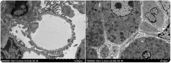
Left: Mouse kidney. Right: Mouse liver. Image Credit: Hitachi High-Tech Europe
In-situ testing
Many accessories and options are available to allow in-situ experiments in the TM4000 II system. These include in-situ stages for rotation, tilting, compression or tensile testing, electrical probing, sample manipulation, heating, cooling, nanoindentation, fatigue testing, etc.
Tensile test in SEM using Deben tensile tester
Example of tensile testing in the SEM, in this case of a leather sample. Video showing a Deben tensile test option. Video Credit: Hitachi High-Tech Europe